A Day in the Half-Life
A Day in the Half-Life
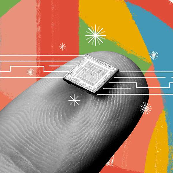
More Microchips, Moore Problems
Use Left/Right to seek, Home/End to jump to start or end. Hold shift to jump forward or backward.
A podcast episode about research and development of microelectronics.
The race to make smaller and smaller electronic chips is coming to an end, after many decades of creative engineering. Individual transistors are now just a few nanometers (that’s billionths of a meter) in length, so there’s not much more shrinking to be done. But there is still a lot of room for improvement. The 20th century effort to pack transistors onto tiny silicon wafers transformed clunky, heavy early electronics into the sleek, portable devices we see today. The challenges of the 21st century will be to make these microelectronics energy efficient and to push the boundaries of what’s possible in a world increasingly integrated with technology.
This episode's guests are Sinéad Griffin and Ramamoorthy Ramesh
Aliyah
This is A Day in the Half-Life. I'm Aliyah Kovner, and in this episode, we're talking about microelectronics.
Ramesh
What is microelectronics? Uh, every time you use your cell phone or you open up your computer to pay your bills, you're using microelectronics.
Aliyah
That is Ramesh, a professor of physics and material science at UC Berkeley and a faculty senior scientist at Berkeley Lab in the Energy Sciences Area.
Ramesh
They have various names. Some people call them chips. Uh, some people call them microprocessors and they are electronics-based components. They think for us, they do logic operations for us, they store information, but all of them are doing some things to better human kind, they're making our life better. And of course, underneath that, there is a whole lot of engineering. There's a whole lot of materials. And at the, at the core of it, whole lot of physics,
Sinead
Right, I think we'd be hard pressed to think of something that doesn't involve microelectronics.
Aliyah
And that's my other guest Sinead Griffin. Sinead is a staff scientist in the material science division and in the Molecular Foundry also at Berkeley lab.
Sinead
So it is, it is the computer that helps us figure out, you know, what, what we're going to, how we're gonna schedule our next doctor's appointment. Everything that has a computer inside. It relies on microelectronics. And in this increased seeing time where we're, uh, more focusing on internet of things, having smart homes, having even our car systems that are now computer based, we're gonna be increasingly reliant on microelectronics to, to navigate the world and to also increase the quality of life for, for day to day life as well.
Aliyah
Welcome Sinead and Ramesh. Let's start at the beginning. I looked up examples of famous electronics from long ago for comparison and the Apollo guidance computer, which is the computer that allowed the Apollo 11 crew to navigate to and from the moon had the equivalent of 0.004 megabytes of editable memory. And it was two feet long about one foot high and it weighed 70 pounds. Um, these days, as you both know, memory chips can be smaller than one square inch and store a terabyte of memory. So when and where did the microelectronics revolution begin?
Ramesh
Great question. Great question. Let's begin at the beginning. <laugh> uh, in, in many instances, microelectronics started at be labs with a few physicists. All of them are Nobel who were all Nobel laureates, uh, asking the question, how do I understand the fundamental properties of matter Sinead? Perhaps you have some insights on it being, uh, a theoretical physicist.
Sinead
Yeah. So, so it was John Bardeen who first really thinking about how we move charges around in a new type of material at the time, which is called a semiconductor. So these are materials that are somewhere in between a good metal and a good insulator. So that that's kind of sounds like it might be contradictory. So an insulator is something where charge doesn't move freely and a metal is one that does. Um, and so it, they were really interested in, in the fundamental physics of these types of systems. They had no idea that this would be so, uh, so for the next technological revolution, they were really just scratching their heads and figuring out, well, these are really interesting materials. Let's try and figure out how they work.
Ramesh
Yeah, exactly. So this started with people just asking simple science questions. This is, uh, winding the clock back to the late forties, early fifties in, in the research environments of places like Bell labs or IBM’s TJ Watson or the Xerox park research centers. And, uh, to a large extent, the national labs with people just asking simple science questions, how do I understand the world around us? But it's soon was clear that this transistor or a transferring of a resistor or at tunable resistor, that's really what it is. So it's a material whose resistance can be changed significantly by several orders of magnitude, actually by applying an electric field to it. And that was the birthplace and the genesis of notion of a transistor. Now, um, fast forward from Bell labs in the early fifties, uh, to the birth of Silicon Valley in the bay area, Silicon Valley did not exist in the fifties.
Ramesh
It was just about ready to be germinated. What happened was there was a huge push to take these ideas and turned them into, uh, technologies that could be productized and sold everywhere. This led to the boom in venture capitalism in Silicon valley. And one of the earliest companies was Fairchild semiconductor, which again was founded by a few people who left Bell labs and who came to the bay area to start thinking about how to productize these ideas. Some of them, uh, then subsequently left to form the company that we know today as Intel. And so there was this whole bunch of, of companies that, uh, mushroomed up all the way into the eighties, uh, when people were using these transistors in a very complicated form, one of the big stepping stones in this was the notion of an integrated circuit. So typically you don't do much with a single transistor. You need a whole bunch of transistors, millions or billions of these transistors working together, both to store information and to do logic operations. So the, the, the advent of the integrated circuit was an important stepping stone.
Aliyah
So one term, I hear a lot when researching microelectronics or reading news about this field is Moore's law. Can you tell me what this means and how it relates to electronics industry?
Sinead
Sure. So, um, Moore’s Law is named after Gordon Moore, um, who was an electronic engineer and in the sixties, he, he noticed that the size of the number of transistors that could fit, uh, was actually increasing every year and a half. So he had had several data points and he fit a line to the data points and made this prediction that the, the, the transitory scaling would follow this law. I think he originally said doubling every other year, but I think it's 1.5 is now, is now, um, where, where that, that scaling law behaves.
Ramesh
Right. It turns out, uh, this is not a fundamental law of nature, but it was more of a techno-economic law. It's exactly like building a high rise apartment. The more, uh, smaller the, the apartment is the more number of apartments that you can build in a given space. So if your chip sizes are one by one centimeter, and if each of these transistors shrinks by 50%, you can build more transistors into the chip. And that meant that you can make different kinds of products. That's where the economic part of it. So this was really a prophecy, a self-fulfilling prophecy that Gordon Moore and that folks in the industry were saying, Gordon Moore, of course, one of the co-founders of Intel, they were, they were pushing it and they were trying to use it as way to push the engineers to innovate some more.
Ramesh
Now this Moores law of course, has been propagated for almost 50 years. And today those length scales are not microns, but nanometers, perhaps we should define length scale a little bit more. Um, it's the critical dimension. What is the dimension of a certain object on the chip? In this case, it's a dimension, a lateral dimension of the wire that carries the current back forth. And in olden days in the sixties and the seventies, they used to be of the order of several micrometers. And people said, okay, I can shrink it by 50% and I would still be okay today.
Ramesh
It is not micrometers. It's nanometers. More importantly, it is of the order of a few nanometers, which means we are reaching the limits of how finally you can cut up the transistor. And this is essentially a, a, a stumbling block or it's, uh, it's a limiting function on Moore law that also therefore says, how does one deal with the next generation where I cannot shrink anymore?
Sinead
Right. Yeah. So, as we come to this limit, as we come to the limit where we're in the nanometers range, where we are really talking about tens of atoms thick at that stage, there's not a lot more clever engineering or fabrication can do, right. We really need to fundamentally rethink what the constituents of these types of areas are and how we can increase their efficiency rather than just make them smaller and smaller and smaller. So we need to start thinking about new physics. We need to start thinking entirely rethinking about what are the fundamental components about how these, how these chips without just reducing the sizes of the individual components anymore.
Ramesh
Sinead, you brought up a very, very important point in the sixties, all the way up to maybe 2010, the focus was on reducing that, that dimension and ergo to follow Morris law or to fulfill Moore’s prophecy. Things worked very well, but in parallel, these chips were consuming a lot of energy. Indeed. Uh, there are predictions, uh, both from Lawrence, Berkeley lab and other, uh agencies, the semiconductor research corporation. For example, they have predicted that if we don't do anything to the total amount of energy, that's consumed in these chronic components by 2030, at least a quarter of the total worldwide energy could be spent in electronics. That's a staggering number today. It's about five to 6%. And so we are not paying much attention, but we let this go with machine learning, artificial intelligence, all of this macroscale phenomena, we could get to a point where a significant amount of our energy is spent in electronics. And therefore there is now this realization that one needs to not only think about defining smaller dimensions, but one also need to reduce the energy consumption in this process, i.e., make it very energy efficient. And this is where Sinead was talking about new physics, new materials coming in.
Sinead
Yeah. So that brings in a whole new challenge to what the fundamental physics and the fundamental mix materials that these types of transistors rely on. Um, so we do have some ideas about how to do this. Um, one of the, uh, and, and to bring it down to really fundamental science, one of the ways we can increase how these transistors work is by including something called spin. Uh, so usual transistors rely on a property of the electron called its charge, and the charge can be moved by electric fields. However, if we include the spin degree of freedom, we can also think about magnetism and, and shuttling around these electrons, using magnetic fields. However, that process requires a of energy. So we, we're gonna ask a different question. Well, what if we can move this spin around with electric fields, that's a much more energy efficient process. So this brings us to the challenge of designing new types of transistors, where we can control the spin with electric fields rather than with magnetic. And these, this isn't, this isn't a dream. These materials do exist. These, these properties do exist in real materials.
Aliyah
So, thank you both that just dovetailed perfectly with, with my next question, which is, you know, what are the problems with the microelectronics industry today? Because as you're both just discussing, you know, the revolutions of the past enabled huge advances in personal electronics and in research, uh, based electronic tools. So, um, Sinead, you described a little bit about the work you're trying to do in this domain to improve microelectronics. Ramesh what are the research community and computer industry doing to take microelectronics beyond Moore's law?
Ramesh
Yeah, that's a great question, Aliyah. So it's like, uh, any other large complex system, all the components of that system have to come together. If you want to have a great, uh, uh, symphony, each of the musicians has to come together, uh, in, in unison to make it work. That's true for microelectronics too. Therefore there is a whole range of translational science that needs to be done all the way from the fundamental signs that places like LBL are so good at, from there to get to a product, there are six degrees of separation.
Ramesh
Each one of those separation steps have to be overcome. For example, in the case of the materials that Sinead is talking about, one has to be able to, to put them down on a large wafer and today's state of the art is a 300 millimeter, a 12-inch wafer. And that's what people like Intel, uh, are working on. So these materials have to be put down on those kinds of platforms. That really means that there needs to be a synthesis process. Then the next question is, does this new device function like the way we take should the physics says it should function, but does it really function, which is really, uh, an issue of measuring these systems.
Ramesh
Then the ultimate part of this is does it function reliably? I mean, does it function for 10 years? Does it store the information? So degradation mechanisms are a very key part. Then the last part of fit, you go from science to technology to markets. The last part of it is how costly, or how cheap is this product? How competitive is it with other technologies that are showing up in the marketplace and is there a different way to solve this problem? All of these things are coming together at the end where you as the consumer or the customer, you don't want to pay any more than what you need to, to get the services or the product that you want. So those are the various steps that a company like Intel will have to, to face taking a new idea, a new concept, like manipulating spins with an electric field all the way into a real product.
Sinead
Yeah. And, uh, the last point you bring up about cost is actually something that can influence us from the very beginning. So when we are designing these types of materials, we can ensure that we don't include very rare, costly elements in the types of materials that we're proposing. So even the very end process of market can actually influence us from the fundamental materials design as well.
Aliyah
That’s really cool to hear just because, I mean, I, I learned all about energy storage in a previous episode, and one huge issue with lithium ion batteries, which the world is now very dependent on is the cobalt and nickel mining. So it's very cool, able to hear they're sort of already considering that before these next generation microchips are born. And I also have been loving hearing about how many different, um, fields of expertise come into both of these. And that's always a great theme for Berkeley lab, which is all about team science. So I would also love to hear just about how you both collaborate with other groups and how, how multidisciplinary this work really is.
Ramesh
Great point, great point Aliyah. So let's, let's pick up on that thread, uh, indeed this whole business of microelectronics, it spans the entire spectrum from the fundamental sciences. We can start with physics, chemistry, uh, mathematics to the engineering sciences, through material science, into electrical engineering, and then pass that to computer science and computer engineering. And it's a huge area of not only research, but business globally. It's about a $500 billion industry, growing at about 18% every year. And therefore the business, uh, aspects of it are, are a key component. Now, uh, um, one of the things is that we are innovating on this is based on a recent program that the department of energy has funded us on is called co-design. You know, in the past 30 years ago, people who did the materials and physics, uh, typically in the universities or the national labs, they worked in their own framework, but they didn't necessarily talk to the people who are making the devices and the people who made the devices perhaps did not talk to the people who are doing the algorithms and everything.
Ramesh
But then we said, Hey, would it not be better if we brought all of them together to work under the same roof? And this is the, the notion of co-design where all of the components, all of the competencies together to solve a big problem. And indeed our co-designed platform is called atoms to architecture. You know, someone like Sinead, who is a theorist who works on, on the fundamental physics of these new materials, somebody like myself, where I make materials and probe their properties. Uh, I am taking all the theoretical knowledge from Sinead and I'm trying to make these materials and probe their properties, but then there are other parts of our team where they're building circuits out of it and they're even higher. Uh, one of our colleagues is looking at how the, the, the notion of artificial intelligence can be used to feed back into designing a better, uh, chip for the future. So the notion of a core design is a confluence of all the disciplines, and this is becoming more and more popular, uh, in the microelectronics business.
Sinead
Yeah. I could probably give a concrete example of how that works at LBL. Um, and I'm gonna talk about the theory since that's the part I'm most familiar with. So, uh, my group looks really how atoms can be combined to give you new types of physics. So we're really in that nano scale, uh, length scale, when we're talking about the fundamental physics of these materials. And typically we wouldn't really discuss much with people who, who design devices. That's just not normally a conversation that happens. Um, <laugh>, they're usually sitting over in a different department, electronic engineering or computer science somewhere else. Um, but what, what this program we have at LBL is doing is forcing us to talk to colleagues that maybe we wouldn't talk science with before. So for example, in, in the microelectronics, we're calculating the, the properties of these materials, we're understanding how to control their behavior.
Sinead
And then we're giving the, uh, the quantities and the properties that we're calculating from an atomic scale up one level, the length scales. So we're giving the properties of these materials, um, to our colleagues in the computational sciences division, who can do larger scale simulations, um, of different types of features, different types of, of, um, combinations of, and geometries of materials to figure out then how these specific materials in interact with each other and perform in, in small devices. And then following that, so following this kind of small device simulation, then they're going to feed it into the architecture. So we really have this atoms to architecture simulation that can then hopefully do the reverse as well. So we can do the reverse project where, you know, the architecture, people say, this will really improve the performance if you can make this modification and that modification.
Aliyah
So, one thing I'm curious about is you both, um, you both have different focus areas, and yet you kind of overlap and you work together on this program, but I'd just like to hear a little bit about what, um, kind of a normal day in the lab or at work is like for each of you when you're not, you know, teaching students or appearing on a podcast, um, what does your, like, hands on work look like?
Sinead
Sure. So we, we use theory and, um, computational techniques to understand and predict new materials and, and new types of physical phenomenal. Um, so there is a lot of, of figuring out different equations, you know, writing things, pencil and paperwork, writing, working things out on blackboards, and then doing a lot of, uh, computational simulations as well. So, uh, a lot of the work is either on the computer or on pencil and paper when we're actually figuring out the equations and figuring out how these systems work. Um, but of course, a big part of it is, is, is, is discussing with colleagues. So meeting and, and figuring out, um, where our mistakes are, how to interpret results and, and meeting with collaborators. So meeting with people like Ramesh, who are physically making and characterizing, uh, and understanding these material reels in, in the actual laboratory rather than inside our computers.
Aliyah
That sounds very cool. And it sounds like your work is, is a little bit more, as you said, pencil and paper a little more, um, cerebral, and I'm wondering Ramesh I, can you in a, uh, clean room suit, bunny suit, gloves, goggles, everything, are you ever going into a fabrication room like that is that part of your day?
Ramesh
Today, for Ramesh personally, that was many moons ago and <laugh>, I'm a professor and many professors don't actually go to the lab to make the things <laugh> why ago, 15 years ago, I used to do this, uh, but my students probably will not let me into the lab because I could be very dangerous. But, uh, we are indeed, as Sinead mentioned, we are experimentalists, which means we make the materials, but we have the power to make these materials by precisely putting one atom at a time, you know, we can make these, uh, very, very perfect quality materials. Indeed. That's a big forte for us in terms of making model systems, understanding, uh, at the core, what the properties look like. And that's how, how we kind of tag team with Sinead, who is a theorist. She makes the predictions, we make the materials and we ask, do these match up, are there differences? And that, so there's a lot of back and forth discussion. Sometimes they very intense discussions because we are all very animated science people <laugh> then the next part of it is we have to go do the measurements of these, and that requires capabilities like the national center for microscopy or advanced light source, where you can do some of the most sophisticated measurements to probe the properties of these kinds of new materials that we make.
Aliyah
What does creating a sample? Um, actually look like. I, I mean, for me, I can't even really picture what kind of machines would be involved or, you know, what is involved in that process. If possible, could you describe that?
Ramesh
Yeah. So, uh, very simply it's like making a sandwich <laugh>. You can make as, as complicated a sandwich and literally it is the same, but it, there is a parallel universe. It looks very much like making a sandwich and let's go through the process. You take a piece of bread for that piece of bread is called a substrate. That's typically a Silicon wafer. Okay. And you stick it on a surface. Typically I don't like a cold sandwich. I, I like a hot sandwich, so I toast, uh, my bread. And instead on a substrate, we heat it up to high temperatures because that's how you make the right kind of material. So you have the bread that's toasted. You put the first piece of cheese. That could be one of the layers in the material, which we would evaporate, uh, cheese. You don't evaporate. You just put it on from, uh, from the slice for us, we would evaporate.
Ramesh
But the key difference would be the cheese is macroscopic. You know, it's a few millimeter thick slice in our case, it's one atom, one atom at a time. And therefore we can basically place these atoms. We have, uh, techniques that we call molecular beam epitaxy and each of those looks like a heavy technical word, and they are, uh, we can take atomic beams, and and spray them, you can think of it as spray painting, but the atomic scale, and you can position the atoms on a surface almost completely precisely. And then you, you say, okay, I built one layer. I put the cheese down, I now put a piece of tomato on it. And the piece of tomato is my active layer, the one which I want to manipulate, and I can, I can come back with a technique, uh, like these deposition techniques, a chemical vapor, uh, based approach or a physical vapor approach and put down the layer ABI and in doing so we can essentially control the properties at the atomic scale.
Sinead
I, I think that that analogy is great as, as well as describing the role of theory. So in theory, we can see, is it better to put down the cheese or the tomato first, or maybe we need to add some pickle in there to make it a full sandwich damage.
Ramesh
That's right. Yeah. But theory will also tell you what is the, the, the right kind of, uh, cheese and what is the, uh, right thickness of the tomato, uh, that gives you the best sandwich? And no, uh, two sandwiches are made the same, and your right that theory is, is that, that very important design glue that makes it all come together.
Aliyah
The production process for these new microelectronics sounds really interesting. And you are thinking about new materials to use for them, but how do you decide what kind of cheese to use, or of figure out what the best new tomato is that the world needs, but they've never had yet. How, how do you do that?
Sinead
Sure. So, so for the particular type of material that we're interested in, these, these are called multiferroics or magneto-electrics. They're actually really rare. Uh, so they, they were first, uh, measured and over, you know, a few decades ago, but really were serendipitously discovered until recently. So it was really on this sort of Edisonian case by case basis where we accidentally stumble across a material that has these properties, and then we try and understand why it's working. Um, and actually that led to my, my PhD advisor, Nicola Spalding actually wrote a paper in 2000 that explained why these are so rare. Um, so the types of, of chemical properties and chemical motifs that you need for something to have these types of functionalities is actually really rarely occurring in the same materials class. Um, however, recently we've been able to rethink the materials discovery process, um, with the advances of large materials databases, like the Materials Project. So in, in the materials project, we've got over a hundred thousand inorganic crystals. And rather than, you know, going through, or Ramesh through each material on a case by case basis, I don't know how long it would take him to do a hundred thousand materials. You probably need a few more grad students. Um, you will
Ramesh
A few more lifetimes more like! <laugh>.
Sinead
<Laugh> Um, so rather than, than doing it on this case, by case basis, we can actually search these large databases for specific properties and constraints to allow us to make new predictions of materials that have the properties that we want. So it's really, uh, going through this, this materials, discovery process in a whole new way, by starting off with a very large selection of materials, and then being able to down select and pinpoint the exact ones that we need for these types of applications.
Aliyah
Is this platform available to, uh, scientists outside of Berkeley lab?
Sinead
Yes. So it's, it's free and openly available. So mm-hmm, <affirmative> www.materials. project.org will get you there. There's also an API, so you can make API requests as well, um, of the materials project also.
Ramesh
Yeah, exactly. I think, uh, you can, now the computers are so powerful that they were not so 20 years ago, they're so powerful that you can basically design everything in your computer, including the chip and the computer itself. They are so powerful. And so you can say, “Hey, computer, tell me what's the best way to, to go about discovering this.” And the computer will go through, look at a hundred thousand different, uh, uh, compound and say, “Hey, look, focus on these 10. This is the best chance that, that you got to meet your own specs that you want to meet.” Then you go back to the experimental and say, guys, I think this is going to work. If you pick this chemical species, mix it this way. And bingo, you got a great sandwich, you know, and this is really the power of the materials project that she’s involved in that you now have completely transformed materials discovery.
Aliyah
Are any of these multiferroic materials that you're working with, are any of them naturally occurring or were, was the class of material in itself kind of designed in the lab?
Sinead
So many of them are found naturally. Um, but the, the ones with the best properties generally aren't, so they generally require some sort of modification, whether that is thinning them down to being only a few layers thick and stacking them into sandwiches, or maybe introducing some new element into the material to enhance one of the properties,
Ramesh
Right. Uh, actually one of the systems, uh, we, we always make a joke out of it, uh, that she made myself and, uh, Nicola Spalding, who's involved in our project as well is, is made out of bismuth, iron, and oxygen, bismuth iron oxide. And we joke that if you have a stomach ache, you can take some bismuth iron oxide. It's like pepto bismo, you know,
Aliyah
I love, I love bismuth, <laugh> I rely on that stuff.
Ramesh
<laugh> Mmm-hmm <affirmative> Or if you're anemic, uh, you should take some bismuth iron oxide. It's got iron in it, you know, and so iron, of course, it's a very primordial element. It's a very, um, pervasive element in the universe but they have to be put into a certain state, you have to constrain them in a way that you get the best performance out of them. That's where you transit from fundamental physics to engineering, because you're, you are now saying, I need to meet certain specifications.
Aliyah
So I'm so curious now, um, you know, you're actively working on designing new chips that have new materials with new properties, you know, going beyond the traditional semiconductor materials that we use today, but once you have a chip like that, um, is this gonna something that could kind of be dropped in, in place where traditional microelectronics are now, or would it sort of necessitate a change in the larger systems as well? Like, can you just swap it out or is it gonna be more complicated than that?
Ramesh
This is a great question, Aliyah. This is a great question. So of, uh, to give our, uh, listeners a perspective, one of the big issues, if you remember a few minutes ago, I mentioned cost. It turns out that these microelectronic chips have to be made under very, very clean conditions. And therefore you will hear from people that it takes 20 billion to build one of these factories. Hmm. So the fab managers in the microelectronics will not let strange materials come in. And therefore this is a really important issue, uh, compatibility. And I, I always give this example if you're a vegetarian for some reason, right? You don't want somebody to come into your kitchen of chicken because that will mess up. It's not vegetarian, similarly fab managers like their kitchens to be very clean because their livelihood depends on it. So because of the cost involved, uh, not tens of billions of dollars, it is not a trivial thing to bring in new materials.
Ramesh
So there's a lot of thinking, lot of pretesting that happens before you can take some of the exotic new materials that we are talking about into a fab. Having said that we know that the fabs have also become more and more progressive in their thinking and more accepting of new materials that 20 years ago they would not. And the prime reason again, is the fact that they're ending, they're coming to the end of Moore’s law. They need more innovation, which will be enabled by new materials. So, yes, in principle, uh, there are companies that I know of who are doing this already, who are taking new materials, complex materials and dropping it into a standard silicon-based platform.
Aliyah
And would the resulting, um, chips be ready to swap into today's electronics? Like say a, a phone, or would the phone have to be re-engineered to accommodate that new technology?
Ramesh
Yeah, great question. Again, most of them, most of them are drop in the sense, the system, which is the phone or your communication system or your computing system is already there. And so they will be a minimal amount of, uh, of disruption to the existing system. Now, having said that, imagine that you com came up with a completely new architecture, the neuromorphic architecture that may require a complete re-engineering of the system, but that's how progress is made. Anyway, uh, we make big discoveries at the fundamental level, and one of them, a few of them completely changed the landscape all the way to the system level.
Sinead
These neuromorphic, uh, devices are heavily inspired by how our brain works. Oh. Um, so we already know that our brain does a lot of computations very quickly and with very, very efficient use of energy as well, where our brains don't heat up too much when we're doing these computations <laugh>. Um, and so a lot of the next generation microelectronics are using this inspiration of, uh, how brains compute and, and move and process to design the next generation of, of microelectronics as well. So that's where the neuromorphic comes from. It's, it's this kind of brain inspired, um, uh, circuits.
Aliyah
So Sinead, I've heard that you have some very interesting, uh, projects in the works for using these new and improved microelectronics for, for new new areas of research. Can you tell us a little bit about that?
Sinead
Oh, sure. So, um, I I'll start off with how I got interested in, in, in these types of materials in the first place, and it wasn't yes. To solve the energy challenge in microelectronics. I will be honest <laugh>, um, it, it, it was, it was because, um, I, I saw picture of these materials. So images that have been taken by an experimental collaborator, uh, Manfred Fiebig who's at the ETH Zurich in Switzerland. And, and these were really cool images of these black and white swirling domains. And so domains are areas of the material that have similar properties and, and these types of materials, form domains, and for of these nice, uh, they kind of look like psychedelic sixties types of pictures with these swirls <laugh>, uh, but at the time they didn't know why these patterns were forming that the way they were.
Sinead
Um, but I had previously done work on cosmic string formation in the early universe. So during the big bang, right after the big bang, the universe had lots of phase transitions as it cooled. And the, the properties of the structure of space time changed during these phase transitions. And one of the predictions for one of these early theories is called the Kibble-Zurich mechanism said that giant cosmic strings forms during these phase transitions and would separate these different types of domains. Um, so we looked at these, these materials that are really interesting for microelectronics now, um, to see if the theories that just these big bang theories could be applied to describe these pattern formations in, in, in these multiferroic materials, and it, it worked. So we predicted that the, the formation of, of these patterns could be described using the formation of cosmic strings in the early universe. [Wow.] Um, so not, not exactly, um, applied to <laugh> to this problem of energy reduction in microelectronics, but, but still, um, really trying to understand the fundamental physics and chemistry of these types of systems.
Aliyah
That's amazing that the, that physics of things on the largest possible scales could relate to things on the smallest, is really interesting work. And so, um, is that, those strings and those patterns in the early universe, um, is that, is that related to, the theory of how the universe got, um, basically clumpy and why there's some areas where there's stuff and some areas where there's nothing, or is that something totally different?
Sinead
So this, these predictions of, of cosmic strings, they're called topological defects, that's the, the technical phrase for them. Um, actually, so we're able to look at the cosmic microwave background, right? So we're able to kind of visualize the constituents of, of the universe and see if there are any regions where we get matter or energy clumped together. So they've actually discounted much of the universe being comprised of these types of cosmic strings. Um, but what we were able to do when we looked in this real material on earth to check to see if the physics was correct. So even though this prediction had been made that these cosmic strings should for during the big bang, uh, no one had way you couldn't rerun the universe, right. We can't rerun the big bang to check, to see if, if the physics is right, but what we can do is rerun the experiment on the material in the lab. And so that's what we're able to do is check that the physics was right and checked that the equations held in, in a real system.
Aliyah
And is this work ongoing or are you working on something different now?
Sinead
So we have mostly, well, I have mostly finished off that work. Um, but there's still a lot of open questions that I'm, you know, that are still, um, hanging out at the back of my brain on, on that project. Um, one of the findings we found was that when you, when you cool a material really, really quickly, uh, we get a different domain formation that what the theory would expect, and that's something we haven't been able to solve yet. So that's something that is still, um, keeping me up at night sometimes, and, and waking me up in the middle of the night. But, um, in general, that, that most of the work I've done on that is, is already out there. And, and you can read about it.
Aliyah
Wonderful. Um, so I think we don't have too much time left. So one thing I would love to cover kind of, uh, before we wrap up is, you know, you, you both have very interesting careers and you're both attacking problems from different perspectives that are very complimentary, but I just wanted to hear a little bit about how you both came into your roles and sort of your personal course, uh, as a scientist, how you got where you are today, and if there were any interesting or unexpected moments along the way.
Ramesh
Okay. Sure, sure. Yeah. Oh yeah. There's life was full of, uh, Bollywood dance dramas and fight sequences and unexpected twists and stuff. But in my case, you know, I did my PhD here at Berkeley a long time ago, and I was gonna stay here at LBL. I got this very strange offer, this was back in the late eighties, from Bell. And, uh, my advisor said, oh, I can't afford to pay you that much. So I went out to New Jersey <laugh>. It was a fantastic experience. We discovered many things. And then I went to Maryland. Uh, University of Maryland for nine years, came back to Berkeley in 2004. But for sure, I, I can, I can see at least four different points or things that happened that dramatically changed. One of them was, um, this discovery of something called colossal magneto-resistance.
Ramesh
This was a project that we literally worked for seven days without sleeping. Hmm. And it was, it was a big discovery at that time, opened up a new field back in early nineties. And, uh, I remember this because I was one of the people growing the material. Uh, the second one was, of course, the material that Sinead was talking about, uh, we were doing something else. We were looking at other materials called ferroelectrics. These are like your kitchen magnet, but, um, they are electrically that way, not magnetically. Oh. And so one of my colleagues was telling me about coupling between magnetism and electricity. I said, yeah, I've heard of Maxwell’s equations and stuff like that, but I wasn't paying attention.
Ramesh
But we, at that time, this was back in the late 1990s, we had stumbled onto a material, which is now a very popular material, uh, in, in the condensed matter community, which has this attribute that it has both magnetism and a electricity, and you can manipulate the magnetism within an electric field. These are the multiferroics. Now it turns out that I, I work very closely with Sinead’s advisor, former advisor, Nicola Spaldin, who did some of the early theoretical work with us. In between, I did a lot of other things. I went to DOE I spent two years in the department of energy, leading something called the sun shot initiative. It was the, the entire solar program for the United States.
Ramesh
Oh, wow. We had an amazing team of people there, again, this works because you bring the right set of people together. We had Steve Chu, who was an energy secretary, and stuff like that. Uh, but basically, uh, Sun shot defined how to bring the cost of solar down to a parity. And for me, it was an eye-opening experience because that was the first time that I had seen research at the macroscopic level, meaning – and now this is a very key underpinning for my own research -- where you can take a macroscopic global problem, something which is at the trillions of dollars in, in terms of markets, you can cascade down all the way to fundamental physics. And so that was an amazing experience, uh, learning a lot. Then when I came back to LBL, uh, as an associate lab director for energy technologies, we used that idea, how do you make these connections? Now? They seem very far away, but if you make the connections, uh, something very special could happen. And so that's been my, my learning pathway.
Sinead
So I actually was originally gonna go to art school. So I started off in a complete <laugh>. I started off completely on the wrong track, I guess. Um, and my, my art teacher said, you know, you should probably do physics. And I don't know if he, if he was being, entirely nice about that when he said you should be a physicist rather than an artist. But, uh, I, actually originally was gonna be a string theorist. I thought I wanted to do high-energy physics. And I ended up, uh, I, I grew up in Ireland in Dublin, and I went to university in Trinity college, Dublin. And I got really lucky that I got an internship in UC Santa Barbara when I was in my third year. And I chose UC Santa Barbara for the internship, because it, it, it was a lot warmer and there was a beach nearby and we don't have, we don't have weather like that in Ireland.
Sinead
Uh, but the other lucky thing of out that was I got to work with, um, uh, a professor there, who was a professor at, in Santa Barbara at the time, which is Nicola Spaldin. And that was pretty pivotal in my, in my career, in one: in convincing me that solid-state physics research was really where the interesting problems that I was interested in were, um, and also, uh, Nicola ended up being my, my PhD advisor later on as well. Um, and I don't, I don't think Ramesh remembers this at all, but when I was, when I was visiting UC Santa Barbara, I, I actually came up to Berkeley one day and visiting you, remember that Ramesh?
Ramesh
Absolutely.
Sinead
Yeah, yeah, yeah, <laugh> as, as an undergraduate. So, there were several factors at play for me ending up in, in this type of, uh, research direction.
Ramesh
Yeah. But, you know, in some sense, physics is one of the, the most beautiful manifestations of art, right? I mean, if you can, to reach deep into yourself and use the principles of physics, you know, these, these boundaries between music and physics and art, you know, Mozart was a mathematician in some sense, right? So these boundaries actually become very fuzzy and that's perhaps the most fun part of doing science that you can look at perspectives, well, be beyond what you're taught in your classes. You know.
Aliyah
Every physicist I've talked to is basically also part philosopher. So it's a good <laugh> of course, it's a good domain for those people,
Ramesh
Of course, it's free. So you can philosophize about anything! But, uh, but I think physics is a way to ponder the universe. You know, I'm learning physics. In my own case, I was not trained as a physicist. I was trained as a material science person. I'm actually going slowly backwards into physics. I figured by the time I'm all done, I would've figured out some parts of physics, you know, which is a, just a beautiful field.
Aliyah
Thank you, Sinead and Ramesh for being here, again, and for talking with me about microelectronics today.
Ramesh
Yeah. It's been a pleasure Aliyah. Uh, of course I talk to Sinead very often because we collaborate on many projects, but this has been a pleasure to be able to have this fireside chat podcast, with you leading us. Thank you very much for the opportunity.
Sinead
Thank you so much. It was, it was, it was an honor and a privilege to, to tell you about the work we're doing at, at LBL. And I look forward to, to hearing the podcast.
Aliyah
Thanks for listening to A Day in the Half-Life on your microelectronics-based device. See you next time.
.png)